DARPA Making Progress on Miniaturized Atomic Clocks for Future PNT Applications
Researchers on the ACES program show early signs of success in developing chip-scale atomic clocks with 1000x performance improvements
OUTREACH@DARPA.MIL
8/20/2019
Many of today’s communications, navigation, financial transaction, distributed cloud, and defense applications rely on the precision timing of atomic clocks – or clocks that track time based on the oscillation of atoms with the highest degrees of accuracy. Harnessing the power of atoms for precise timing requires a host of sophisticated and bulky technologies that are costly to develop and consume large amounts of energy. New applications and technologies like 5G networks and GPS alternatives will require precise timekeeping on portable platforms, driving a demand for miniaturized atomic clocks with a high degree of performance.
Over the past few decades, DARPA has invested heavily in the advancement and miniaturization of atomic clock technology, generating chip-scale atomic clocks (CSACs) that are now commercially available and offer unprecedented timing stability for their size, weight, and power (SWaP). However, the performance of these first-generation CSACs are fundamentally limited due to the physics associated with their designs. Calibration requirements and frequency drift can generate timing errors, making it difficult to achieve the highest degrees of accuracy and reliability in a portable package. DARPA’s Atomic Clock with Enhanced Stability (ACES) program is exploring the development of next-generation, battery-powered CSACs with 1000x improvement in key performance parameters over existing options.
“Shrinking atomic clocks from large cesium beam tubes to chip-scale devices without eroding performance requires a rethinking of a number of critical components, including vacuum pumps and optical isolators as well as new approaches to component integration,” said Dr. John Burke, the program manager leading ACES in DARPA’s Microsystems Technology Office (MTO). “The target metrics we outlined for the ACES program are lofty, but as we enter the third phase of the program, researchers are already demonstrating engineering successes including reduced SWaP, lab-proven atomic clock technologies, as well as early prototypes of future clock architectures.”
Through the exploration of alternative physics architectures and novel component technologies, three sets of researchers have demonstrated early progress towards creating CSACs with 1000x improvement in temperature control, aging, and retrace.
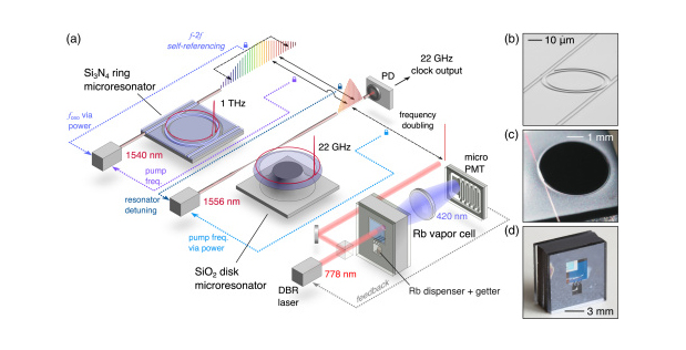
A paper recently published in Optica highlights recent progress made by a team of researchers from the National Institute of Standards and Technology (NIST), with support from researchers at the California Institute of Technology, Stanford University, and Charles Stark Draper Laboratories. The team has demonstrated an experimental optical atomic clock that is comprised of only three small chips and supporting electronics and optics. Unlike standard atom clocks that operate at microwave frequencies and track the vibrations of cesium atoms, optical atomic clocks run at higher frequencies, offering greater precision because they divide time into smaller units. The NIST team’s clock uses a laser to track the oscillations of rubidium atoms confined in a vapor cell – or tiny glass container – that is 3 millimeters across sitting on top of a silicon chip. Within the clock’s chip-based “heart,” two frequency combs act like gears to convert the rubidium atoms’ high-frequency optical “ticks” to the lower microwave frequency, which is used by most PNT applications to track time. In addition to providing a higher-degree of accuracy (roughly 50 times better than the current cesium-based CSACs), the experimental clock uses very little power – just 275 milliwatts.
In addition to successfully demonstrating a chip-scale optical clock, the NIST team was able to microfabricate all of the key components, much in the same way that computer chips are fabricated. This enables further integration of the electronics and optics while creating a potential path towards mass production and commercialization.
Figure 1. Schematic of the microfabricated photonic optical atomic clock developed by NIST, California Institute of Technology, Stanford University, and Charles Stark Draper Laboratories. Source: NIST
A second team of researchers from Honeywell, working in partnership with University of California, Santa Barbara, is developing precision atomic sensors to support the development of a miniature atomic clock.
To date, the miniaturization of trapped-atom sensors has been stymied by bulk optical elements - such as lenses and mirrors - that traditionally compose the necessary optical system. The precision atomic sensors the Honeywell team has developed rely on a magneto-optic trap (MOT), which requires a three-dimensional arrangement of laser beams coming from different directions, precisely crossing at a point. To achieve this precise configuration without the use of lenses or mirrors, the researchers developed an integrated photonic chip that guides light around an “optical circuit” – which is analogous to the guiding of electrical signals in traditional computer chips. The photonic chip emits three large collimated beams of light in the proper three-dimensional arrangement to make a MOT. By combining these intersecting laser beams with a specialized set of compact magnetic field coils, Honeywell used this light source to trap rubidium atoms, and realize an advanced, miniature atomic clock.
Honeywell’s integrated photonic chip technology not only reduces the size, weight, and power of laser delivery systems, but also allows for batch fabrication of complex optical systems with reduced manufacturing cost.
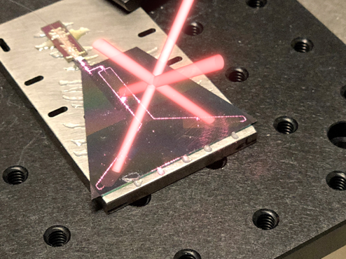
Figure 2. Silicon chip with waveguides and gratings to create a 3D laser beam pattern. In the photo, the light-guiding channels glow from the light they are directing, and the invisible 3D beams coming out of the chip are indicated by a computer-rendered overlay. Source: Honeywell
Finally, a team from NASA’s Jet Propulsion Laboratory (JPL), with support from researchers at SRI International; University of California, Davis; and University of Illinois Urbana-Champaign, has demonstrated an experimental atomic clock capable of meeting ACES’ target metrics, while proving immune to temperature and environmental issues. Building off research that created the Deep Space Atomic Clock (DSAC), the team developed an ion-based approach to atom cooling that relies on ionized mercury and ultraviolet lamps instead of lasers. The JPL atomic clock showed an immunity of less than 1 part in 14 decimal places for 1 degree Celsius change. To put that in perspective, that is about 100x better than current CSACs. The use of mercury ions also provides more stability while making the technology less sensitive to magnetic fields and temperature changes.
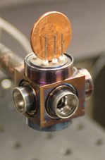
Figure 3. This photo is of the ACES 10 cc package developed by researchers from NASA’s JPL. Source: NASA Jet Propulsion Laboratory
As evidenced by the NIST and Honeywell research, progress on the ACES program is generating new means of fabricating atomic clock technologies at wafer scale, which makes continued exploration more cost effective and less reliant on massive engineering endeavors. “Today, we are dealing with complicated optical systems that require massive amounts of engineering whenever you want to iterate on a design. The early progress made on ACES shows that there are viable options in development for doing this same thing without the massive engineering manpower or hefty costs associated with current approaches,” noted Burke.
ليست هناك تعليقات:
إرسال تعليق